Flow soldering and wave soldering both utilize tin alloys to create reliable, conductive joints in electronic assemblies, but differ significantly in application method and efficiency. Flow soldering employs a controlled molten tin alloy flow directed at specific components for precise soldering, ideal for complex or small-scale production. Wave soldering, on the other hand, exposes the entire board to a continuous wave of molten tin alloy, enabling faster processing of large, through-hole assemblies while maintaining strong, consistent solder joints.
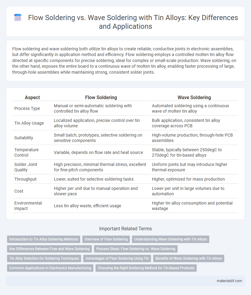
Table of Comparison
| Aspect | Flow Soldering | Wave Soldering |
|---|---|---|
| Process Type | Manual or semi-automatic soldering with controlled tin alloy flow | Automated soldering using a continuous wave of molten tin alloy |
| Tin Alloy Usage | Localized application, precise control over tin alloy volume | Bulk application, consistent tin alloy coverage across PCB |
| Suitability | Small batch, prototypes, selective soldering on sensitive components | High-volume production, through-hole PCB assemblies |
| Temperature Control | Variable, depends on flow rate and heat source | Stable, typically between 250degC to 270degC for tin-based alloys |
| Solder Joint Quality | High precision, minimal thermal stress, excellent for fine-pitch components | Uniform joints but may introduce higher thermal exposure |
| Throughput | Lower, suited for selective soldering tasks | Higher, optimized for mass production |
| Cost | Higher per unit due to manual operation and slower pace | Lower per unit in large volumes due to automation |
| Environmental Impact | Less tin alloy waste, efficient usage | Higher tin alloy consumption and potential wastage |
Introduction to Tin Alloy Soldering Methods
Flow soldering and wave soldering are two primary tin alloy soldering methods used for securing electronic components on circuit boards. Flow soldering involves the controlled application of molten tin alloy, providing precision for small-scale or complex assemblies, whereas wave soldering employs a continuous wave of molten tin alloy to quickly solder multiple joints on densely populated boards. Both techniques utilize tin-based alloys, selected for their excellent wetting properties and reliable electrical conductivity in electronic manufacturing.
Overview of Flow Soldering
Flow soldering uses a controlled jet of molten tin alloys to solder electronic components, providing precise temperature regulation and minimal thermal stress on sensitive parts. This method enhances solder joint quality by ensuring uniform coverage and reducing defects such as solder bridging commonly encountered in wave soldering. Its efficiency in selectively soldering through-hole and surface mount components makes it ideal for complex assemblies requiring consistent tin alloy application.
Understanding Wave Soldering with Tin Alloys
Wave soldering with tin alloys ensures consistent solder joint quality by using a controlled molten wave of solder, typically composed of tin-lead or lead-free mixtures such as Sn-Ag-Cu. This process offers precise temperature regulation and efficient heat transfer, optimizing solder flow and wetting characteristics essential for high-reliability printed circuit boards (PCBs). The tin alloy composition directly influences the solder's melting point, mechanical strength, and resistance to thermal fatigue, making wave soldering ideal for mass production with uniform tin alloy application.
Key Differences Between Flow and Wave Soldering
Flow soldering uses a controlled wave of molten tin alloy to solder surface mount components efficiently, whereas wave soldering employs a continuous wave of tin alloy to solder through-hole components. Flow soldering provides precise, localized heat application suitable for delicate electronic assemblies, while wave soldering offers high throughput for mass production with consistent solder joint quality. The key differences lie in component compatibility, heat control, and production scale, with flow soldering favoring complex SMT boards and wave soldering excelling in PCB assemblies with numerous through-hole connections.
Process Steps: Flow Soldering vs. Wave Soldering
Flow soldering involves directing a controlled stream of molten tin alloy onto the underside of a PCB for soldering components, ensuring precise application and minimal thermal stress. Wave soldering utilizes a continuous, turbulent wave of molten tin alloy that contacts the entire PCB underside, allowing simultaneous soldering of multiple joints, ideal for through-hole components. Both processes require pre-heating, flux application, and post-soldering inspection but differ significantly in solder application method and suitability for component types.
Tin Alloy Selection for Soldering Techniques
Choosing the right tin alloy is critical for optimizing flow soldering and wave soldering processes, with tin-silver-copper (SAC) alloys favored for lead-free soldering due to their excellent wetting properties and high thermal fatigue resistance. Flow soldering typically requires alloys with lower melting points and enhanced fluidity, such as tin-bismuth or tin-indium, to accommodate precise temperature control and avoid component damage. Wave soldering demands tin alloys with robust mechanical strength and oxidation resistance, making SAC and tin-copper-nickel blends ideal for reliable, consistent solder joints in high-volume electronics manufacturing.
Advantages of Flow Soldering Using Tin
Flow soldering using tin alloys offers precise control over solder application, resulting in consistent joint quality and reduced risk of thermal damage to sensitive components. The process enables efficient solder coverage on complex or uneven surfaces, improving reliability in high-density electronic assemblies. Lower tin alloy consumption and minimized solder waste enhance cost-effectiveness and environmental sustainability in manufacturing.
Benefits of Wave Soldering with Tin Alloys
Wave soldering with tin alloys ensures consistent, reliable solder joints by uniformly applying molten solder across entire circuit boards, significantly reducing defects and improving production efficiency. The process excels in handling complex, high-density PCB assemblies where precision and speed are critical, leveraging the excellent wetting properties of tin alloys to enhance joint strength and electrical conductivity. Compared to flow soldering, wave soldering offers superior throughput and reduced labor costs, making it ideal for large-scale manufacturing environments requiring robust, high-quality electronic connections.
Common Applications in Electronics Manufacturing
Flow soldering commonly uses tin-lead or lead-free tin alloys to solder small-surface-mounted components on printed circuit boards (PCBs), providing precision and controlled heat application. Wave soldering, employing tin-based alloys like Sn63Pb37 or SAC305, is ideal for through-hole component assembly and mass production, offering high throughput for electronics such as connectors and power supplies. Both processes leverage the excellent wettability and melting characteristics of tin alloys to ensure reliable electrical connections and mechanical strength in electronic devices.
Choosing the Right Soldering Method for Tin-Based Products
Flow soldering provides precise control over temperature and solder flow, making it ideal for delicate tin-based electronic components with complex geometries. Wave soldering offers higher throughput and consistent solder application, suitable for mass production of tin alloy PCBs with robust through-hole components. Selecting between flow and wave soldering depends on factors such as product complexity, production volume, and tin alloy composition to ensure optimal joint strength and reliability.
Flow Soldering vs Wave Soldering (using Tin alloys) Infographic